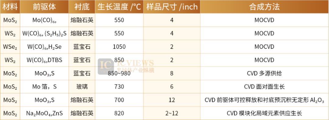
中国二维半导体产业链正加速成型。极钼芯科技基于自主研发的Oxy-MOCVD 200 ultra设备(核心部件100%国产化)于2025年10月报道了全球首个6英寸二维过渡金属硫族化合物半导体单晶量产化制备,150毫米晶圆单向畴对齐率超过99%1。同年发布了全球首款基于二维半导体的32位RISC-V架构微处理器"无极",采用MoS₂材料,集成5900个晶体管,厚度仅0.7纳米1。2026年1月,南京大学与东南大学团队合作开发氧辅助金属有机化学气相沉积技术,二硫化钼晶畴平均尺寸从百纳米级提升至数百微米1。同月,南京大学团队研制出"梦启(MAGIC)-1000"微处理器,集成1433个MoS₂晶体管,晶体管集成密度达9336个/mm²1。
材料制备和存储领域也取得重要进展。中国科学院金属研究所于2026年7月制备出大面积高性能p型MoSi₂N₄单层单晶晶圆1。复旦大学团队打造的二维半导体DRAM实现了超过8500秒的超长数据保持时间,并在2026年7月实现单电子非易失性存储,存储窗口达0.5伏特1。
工程化进展方面,原集微8英寸二维半导体工程化示范工艺线于2026年7月9日在浦东全线贯通,工艺良率大于99.99%,可支撑10万管级二维电路设计与晶圆级制造1。值得注意的是,二维半导体产线可复用现有硅基半导体设备的比例约为70%1。
China's two-dimensional semiconductor industry chain is accelerating toward maturity, with significant breakthroughs spanning material preparation, equipment development, and chip integration.1 In October 2025, Jimu Semiconductor reported the world's first production-scale fabrication of six-inch two-dimensional transition metal dichalcogenide single crystals using its independently developed Oxy-MOCVD 200 ultra equipment, with core components achieving 100% domestic manufacturing.1 The 150-millimeter wafers demonstrated unidirectional domain alignment rates exceeding 99%.1 By January 2026, a collaborative team from Nanjing University and Southeast University advanced the fabrication technology further, expanding molybdenum disulfide grain sizes from the hundred-nanometer scale to hundreds of micrometers.1
Progress in material science has been paralleled by advances in equipment and process integration. In July 2026, researchers at the Chinese Academy of Sciences Institute of Metal Research successfully fabricated large-area, high-performance p-type MoSi₂N₄ single-layer single-crystal wafers.1 The demonstration production line for two-dimensional semiconductors operated by Original Integrated Circuits achieved full operational status on July 9, 2026, in Pudong with process yields exceeding 99.99%, capable of supporting circuit designs and wafer-scale manufacturing at the 100,000-transistor level.1 Approximately 70% of the production line equipment can be repurposed from existing silicon-based semiconductor infrastructure.1
The industry has moved beyond materials and processes to functional chip products. In 2025, researchers unveiled the world's first 32-bit RISC-V architecture microprocessor based on two-dimensional semiconductors, dubbed "Wuji," utilizing MoS₂ material with 5,900 integrated transistors and a thickness of just 0.7 nanometers.1 A Nanjing University team subsequently developed the "MAGIC-1000" microprocessor in 2026, integrating 1,433 MoS₂ transistors with a transistor density reaching 9,336 per square millimeter.1 In the memory sector, Fudan University's research team demonstrated two-dimensional semiconductor DRAM with data retention exceeding 8,500 seconds, and achieved single-electron nonvolatile storage in July 2026 with a storage window of 0.5 volts.1
评论
还没有评论,欢迎留下第一条。